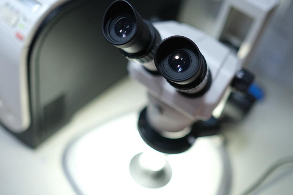
Scanning electron microscopes (SEM) are powerful magnification tools that use focused electron bundles to obtain information. The high-resolution, three-dimensional images produced by these microscopes, which are about the size of 2 people, provide topographic, morphological and compositional information, making them invaluable in a variety of scientific and industrial applications.
Microscope Features
Developed by Professor Dr. Charles Oatley together with help from his graduate students in the 1950’s, the SEM is one of three types of electron microscopy (EM).
Electron microscopes use the same basic principles as light microscopes, but focus on energetic electron beams rather than photons to magnify an object.
The main reason for using electrons instead of light is that although light microscopes vary depending on certain wavelengths, light quality and condition, better results can be achieved in electron microscopy. Of course, electron microscopes also require a vacuum system, a cooling system, a solid / un-moving floor surface, a test chamber free of magnetic media, and an uninterrupted power supply to achieve the best results.
What do Microscope Tests Perform?
Scanning Electron Microscopy provides detailed surface information by tracing a sample in a scanning model with an electron beam. The process begins when an electron gun forms a beam of energetic electrons downwards on the column and onto a series of electromagnetic lenses.
These lenses are tubes that are wrapped in helices and are called solenoids. The coils are adjusted to focus the incoming electron beam on the sample; these adjustments cause fluctuations in voltage, increasing / reducing the speed at which the electrons come into contact with the sample surface.
The SEM operator is controlled by computer and can be adjusted to allow the beam to adapt magnification and determine the surface area to be scanned. The beam focuses on the area where a solid sample is placed. Most of the samples require some preparation before they are placed in the vacuum chamber.
Of the various different preparation processes, the two most commonly used before SEM analysis are spray coating for non-conducting samples and the dehydration of most biological samples.
In addition, all samples need to be able to withstand the low pressure inside the vacuum chamber.
The interaction between the incoming electrons and the surface of the sample is determined by the acceleration rate of the incoming electrons, which carry a significant amount of kinetic energy before focusing on the sample.
When the incoming electrons come into contact with the sample, the energetic electrons are released from the surface of the sample. The scattering patterns made by the interaction give information about the size, shape, texture and composition of the sample.
Various detectors are used to determine the different types of scattered electrons, including secondary and back-scattering electrons and x-rays. Diffraction backscatter electrons determine the direction of minerals and micro fabrics as well as crystal structures.
X-rays emitted from below the surface of the sample can provide information about elements and minerals.
Scanning electron microscopes produce black and white, three-dimensional images.
Image magnification can be up to 10 nanometres, with intense interactions occurring on the surface of the sample creating a greater depth of view, higher resolution, and ultimately more detailed surface picture.
Where is Microscope Testing Commonly Used?
Scanning electron microscopes have several applications in a number of scientific and industry related fields, especially where the characterizations of solid materials are useful. In addition to topographical, morphological and compositional information SEM’s are able to detect and analyse fractured surfaces, can provide information on micro structures, examine surface contamination, reveal spatial changes in the chemical composition, provide qualitative chemical analysis and define the crystal structures. It can also be used in organic and soft organisms, but it must be well stabilized and chemical fixation must be used. SEM’s are not used very often for organic and soft organisms because they do not provide the level of fine and accurate results that they can for scans of solid materials.
Scanning electron microscopes can be the main research tool in areas such as life sciences, biology, gemology, medicine and forensics, metallurgy. In addition, SEM’s have practical industrial and technological applications such as conductivity inspection, production line of small products, and installation of microchips for computers.
KALKANCI’s Microscope Testing
In order to control the suitability, quality and durability of our products, microscope testing in our quality control process provides quality checks at the micro dimension. We ensure procedures for checking, improving and developing our product quality through KALKANCI microscope testing.